

Introduction to I2C
An Inter-IC bus is often used to communicate across circuit-board distances.The name I2C is shorthand for a standard Inter-IC (integrated circuit) bus. Its original purpose was to provide an easy way to connect a CPU to peripherals chips in a TV set. I2C provides good support for communication with various slow, on-board peripheral devices that are accessed intermittently, while being extremely modest in its hardware resource needs. It is a simple, low-bandwidth, short-distance protocol. Most available I2C devices operate at speeds up to 400Kbps, with some venturing up into the low megahertz range. I2C is easy to use to link multiple devices together since it has a built-in addressing scheme. Examples of simple I2C-compatible devices found in embedded systems include EEPROMs, thermal sensors, and real-time clocks. I2C is also used as a control interface to signal processing devices that have separate, application-specific data interfaces. For instance, it's commonly used in multimedia applications, where typical devices include RF tuners, video decoders and encoders, and audio processors.
The physical I2C bus
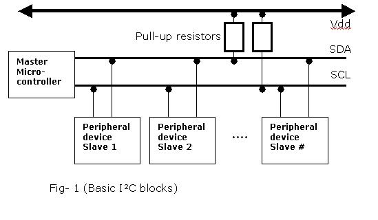
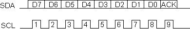
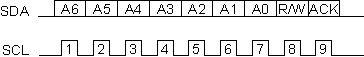
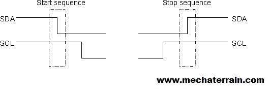
It is a two wire serial bus, called SCL and SDA. SCL is the clock line. Both SDA and SCL are initially bi-directional. It is used to synchronize all data transfers over the I2C bus. SDA is the data line. The SCL & SDA lines are connected to all devices on the I2C bus. Both SCL and SDA lines are "open drain" drivers which means that the chip can drive its output low, but it cannot drive it high. For the line to be able to go high you must provide pull-up resistors to the 5v supply. Together, these signals make it possible to support serial transmission of 8-bit bytes of data-7-bit device addresses plus control bits-over the two-wire serial bus. Data is transferred in sequences of 8 bits. The bits are placed on the SDA line starting with the MSB (Most Significant Bit). The SCL line is then pulsed high, then low. For every 8 bits transferred, the device receiving the data sends back an acknowledge bit, so there are actually 9 SCL clock pulses to transfer each 8 bit byte of data. If the receiving device sends back a low ACK bit, then it has received the data and is ready to accept another byte. If it sends back a high then it is indicating it cannot accept any further data and the master should terminate the transfer by sending a stop sequence.
MASTER AND SLAVE
The device that initiates a transaction on the I2C bus is termed the master. The master normally controls the clock signal. A device being addressed by the master is called a slave. In a bind, an I2C slave can hold off the master in the middle of a transaction using what's called clock stretching (the slave keeps SCL pulled low until it's ready to continue). There may be one or more slaves on the bus. Both masters and slaves can receive and transmit data bytes. The master transmits the device address of the intended slave at the beginning of every transaction. Each slave is responsible for monitoring the bus and responding only to its own address. This addressing scheme limits the number of identical slave devices that can exist on an I2C bus without contention, with the limit set by the number of user-configurable address bits (typically two bits, allowing up to four identical devices).
The I2C Software Protocol
The first thing that will happen is that the master will send out a start sequence. This will alert all the slave devices on the bus that a transaction is starting and they should listen in in case it is for them. Next the master will send out the device address. The slave that matches this address will continue with the transaction, any others will ignore the rest of this transaction and wait for the next. Having addressed the slave device the master must now send out the internal location or register number inside the slave that it wishes to write to or read from. This number is obviously dependent on what the slave actually is and how many internal registers it has. Some very simple devices do not have any, but most do, including all of our modules. Having sent the I2C address and the internal register address the master can now send the data byte (or bytes, it doesn't have to be just one). The master can continue to send data bytes to the slave and these will normally be placed in the following registers because the slave will automatically increment the internal register address after each byte. When the master has finished writing all data to the slave, it sends a stop sequence which completes the transaction. So to write to a slave device:
1. Send a start sequence
2. Send the I2C address of the slave with the R/W bit low (even address)
3. Send the internal register number you want to write to
4. Send the data byte
5. [Optionally, send any further data bytes]
6. Send the stop sequence.
As an example, you have an SRF08 at the factory default address of 0xE0. To start the SRF08 ranging you would write 0x51 to the command register at 0x00 like this:
1. Send a start sequence
2. Send 0xE0 ( I2C address of the SRF08 with the R/W bit low (even address)
3. Send 0x00 (Internal address of the command register)
4. Send 0x51 (The command to start the SRF08 ranging)
5. Send the stop sequence.
Reading from the Slave
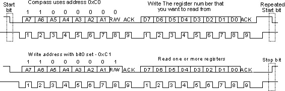
Before reading data from the slave device, you must tell it which of its internal addresses you want to read. So a read of the slave actually starts off by writing to it. This is the same as when you want to write to it: You send the start sequence, the I2C address of the slave with the R/W bit low (even address) and the internal register number you want to write to. Now you send another start sequence (sometimes called a restart) and the I2C address again - this time with the read bit set. You then read as many data bytes as you wish and terminate the transaction with a stop sequence. So to read the compass bearing as a byte from the CMPS03 module:
1. Send a start sequence
2. Send 0xC0 ( I2C address of the CMPS03 with the R/W bit low (even address)
3. Send 0x01 (Internal address of the bearing register)
4. Send a start sequence again (repeated start)
5. Send 0xC1 ( I2C address of the CMPS03 with the R/W bit high (odd address)
6. Read data byte from CMPS03
7. Send the stop sequence.
The bit sequence will look like this:
Category:


