
IC Pin Configuration:
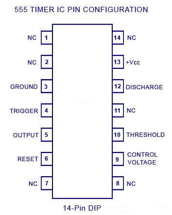
The 555 Timer IC is available as an 8-pin metal can, an 8-pin mini DIP (dual-in-package) or 14-pin DIP. The pin configuration is shown in the figures.
This IC consists of 23 transistors, 2 diodes and 16 resistors. The use of each pin in the IC is explained below. The pin numbers used below refers to the 8-pin DIP and 8-pin metal can packages
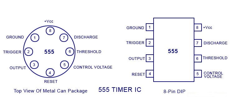
Pin 1: Grounded Terminal: All the voltages are measured with respect to the Ground terminal.
Pin 2: Trigger Terminal: The trigger pin is used to feed the trigger input hen the 555 IC is set up as a monostable multivibrator. This pin is an inverting input of a comparator and is responsible for the transition of flip-flop from set to reset. The output of the timer depends on the amplitude of the external trigger pulse applied to this pin. A negative pulse with a dc level greater than Vcc/3 is applied to this terminal. In the negative edge, as the trigger passes through Vcc/3, the output of the lower comparator becomes high and the complimentary of Q becomes zero. Thus the 555 IC output gets a high voltage, and thus a quasi stable state.
Pin 3: Output Terminal: Output of the timer is available at this pin. There are two ways in which a load can be connected to the output terminal. One way is to connect between output pin (pin 3) and ground pin (pin 1) or between pin 3 and supply pin (pin 8). The load connected between output and ground supply pin is called the normally on load and that connected between output and ground pin is called the normally off load.
Pin 4: Reset Terminal: Whenever the timer IC is to be reset or disabled, a negative pulse is applied to pin 4, and thus is named as reset terminal. The output is reset irrespective of the input condition. When this pin is not to be used for reset purpose, it should be connected to + VCC to avoid any possibility of false triggering.
Pin 5: Control Voltage Terminal: The threshold and trigger levels are controlled using this pin. The pulse width of the output waveform is determined by connecting a POT or bringing in an external voltage to this pin. The external voltage applied to this pin can also be used to modulate the output waveform. Thus, the amount of voltage applied in this terminal will decide when the comparator is to be switched, and thus changes the pulse width of the output. When this pin is not used, it should be bypassed to ground through a 0.01 micro Farad to avoid any noise problem.
Pin 6: Threshold Terminal: This is the non-inverting input terminal of comparator 1, which compares the voltage applied to the terminal with a reference voltage of 2/3 VCC. The amplitude of voltage applied to this terminal is responsible for the set state of flip-flop. When the voltage applied in this terminal is greater than 2/3Vcc, the upper comparator switches to +Vsat and the output gets reset.
Pin 7 : Discharge Terminal: This pin is connected internally to the collector of transistor and mostly a capacitor is connected between this terminal and ground. It is called discharge terminal because when transistor saturates, capacitor discharges through the transistor. When the transistor is cut-off, the capacitor charges at a rate determined by the external resistor and capacitor.
Pin 8: Supply Terminal: A supply voltage of + 5 V to + 18 V is applied to this terminal with respect to ground (pin 1).
Working Principle:
The internal resistors act as a voltage divider network, providing (2/3)Vcc at the non-inverting terminal of the upper comparator and (1/3)Vcc at the inverting terminal of the lower comparator. In most applications, the control input is not used, so that the control voltage equals +(2/3) VCC. Upper comparator has a threshold input (pin 6) and a control input (pin 5). Output of the upper comparator is applied to set (S) input of the flip-flop. Whenever the threshold voltage exceeds the control voltage, the upper comparator will set the flip-flop and its output is high. A high output from the flip-flop when given to the base of the discharge transistor saturates it and thus discharges the transistor that is connected externally to the discharge pin 7. The complementary signal out of the flip-flop goes to pin 3, the output. The output available at pin 3 is low. These conditions will prevail until lower comparator triggers the flip-flop. Even if the voltage at the threshold input falls below (2/3) VCC, that is upper comparator cannot cause the flip-flop to change again. It means that the upper comparator can only force the flip-flop’s output high.
To change the output of flip-flop to low, the voltage at the trigger input must fall below + (1/3) Vcc. When this occurs, lower comparator triggers the flip-flop, forcing its output low. The low output from the flip-flop turns the discharge transistor off and forces the power amplifier to output a high. These conditions will continue independent of the voltage on the trigger input. Lower comparator can only cause the flip-flop to output low.
From the above discussion it is concluded that for the having low output from the timer 555, the voltage on the threshold input must exceed the control voltage or + (2/3) VCC. This also turns the discharge transistor on. To force the output from the timer high, the voltage on the trigger input must drop below +(1/3) VCC. This turns the discharge transistor off.
A voltage may be applied to the control input to change the levels at which the switching occurs. When not in use, a 0.01 nano Farad capacitor should be connected between pin 5 and ground to prevent noise coupled onto this pin from causing false triggering.
Connecting the reset (pin 4) to a logic low will place a high on the output of flip-flop. The discharge transistor will go on and the power amplifier will output a low. This condition will continue until reset is taken high. This allows synchronization or resetting of the circuit’s operation. When not in use, reset should be tied to +VCC.
Pages
Category:


